Saturday, 13 August 2016

Resistors and how to calculate effective resistance?

Resistors are often connected together in a circuit, so it is necessary to know how to determine the resistance of a combination of two or more resistors. There are two basic ways in which resistors can be connected: in series and in parallel.

Determining the total resistance for two or more resistors in series is very simple. Total resistance equals the sum of the individual resistances. In this case, RT=R1+R2+R3 . This makes common sense; if you think again in terms of water flow, a series of obstructions in a pipe add up to slow the flow more than any one. The resistance of a series combination is always greater than any of the individual resistors
                                       .
Some of the total current will flow through R1 and some will flow through R2, causing an equal voltage drop across each resistor. More current, however, will flow through the path of least resistance. The formula for total resistance in a parallel circuit is more complex than for a series circuit:

                                                   RT={1{1R1}+{1R2}...+{1Rn}}
                                                
                                                        Image result for parallel resistance

Friday, 12 August 2016

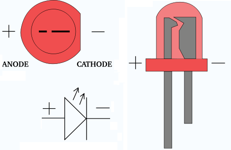
Light Emitting Diode(LED)


What is L.E.D?

ANS.It is a two lead semiconductor light source.It is also P-N junction which emits light when activated.When a suitable voltage is applied to the leads,electrons are able to recombine with electrons holes within the device,releasing energy in the forms of photons.

This effect is called electroluminescence, and the colour of the light is determined by the energy band gap of the semiconductor.

WORKING:


The charge carriers recombine in a forward biased P-N junction as the electrons cross from the N-region and recombine with the holes existing in the P-region.Free electrons are in the 
the conduction band of energy levels,while holes are in the valence energy band.Thus the energy of holes will be lesser than the energy levels of the electron.some portion of energy must be dissipated in order to recombine the electrons and the holes.This energy is emitted in form of heat and light.

Thursday, 11 August 2016

Implementation of NOR gate as universal gate

NOR gate as universal gate

We have seen how NAND gate can be used to make all the three basic gates by using that alone. Now we will discuss the same in case of NOR gate. 


                         Image result for Nor using or

The above diagram is of an OR gate made by only using NOR gates. The output of this gate is exactly similar to that of a single OR gate. As we can see the circuit arrangement of OR gate using NOR gates is similar to that of AND gate using NAND gates. 

                             Image result for Nor using and

The above diagram as the name suggests is of AND gate using only NOR gate, again we can see that the circuit diagram of AND gate using only NOR gate is exactly similar to that of OR gate using only NAND gates. Now we will finally see how a NOT gate can be made by using only NOR gates.

Image result for Nor using NOT


The above diagram is of a NOT gate made by using a NOR gate. The circuit diagram is similar to that of NOT gate made by using only NAND gate. So, from the above discussion it is clear that all the three basic gates (AND, OR, NOT) can be made by only using NOR gate. And thus, it can be aptly termed as Universal Gate.
                                             

How to convert NAND Gate to AND,OR and NOT Gates(Basic Gates)?

     How to convert NAND Gate to AND,OR and NOT Gates(Basic Gates)?


The below diagram is of a two input NAND gate. The first part is an AND gate and second part is a dot after it represents a NOT gate. 
We will consider the truth table of the above NAND gate i.e. a two-input gate. 
The two inputs are A and B.Image result for nand gate
Now we will see how NAND Gate is used to implement all other basic gates .

                                       Image result for nand gate
The above diagram is of an NOT,AND and OR gate made from NAND gate. So we can see that all the three basic gates can be made by only using NAND gates, that’s why this gate is called Universal Gate and it is appropriate.